- Home
- Documentation
- Community
- Projects
- Boards
- Agilex 5 SoC
- Agilex 7 SoC
- Arria 10 SoC
- Nallatech 385A - Arria 10 FPGA Network Accelerator Card
- Nallatech 385A-SoC Accelerator Card with Arria 10 FPGA
- ALARIC Instant DevKit ARRIA 10 SoC FMC IDK by REFLEX CES
- Altera Arria 10 SoC Virtual Platform
- Altera Arria 10 SoC Board
- Nallatech 510T compute acceleration card with Intel Arria 10 FPGA
- REFLEX CES Achilles Arria 10 SoC SOM
- Terasic Arria10 SoC Board : HAN Pilot Platform
- Arria V SoC
- Cyclone V SoC
- Altera Cyclone V SoC Board
- Arrow SoCKit User Manual - July 2017 Edition
- Arrow SoCKit User Manual - November 2019 Edition
- Arrow SoCKit Evaluation Board
- Atlas-SoC Development Platform
- Critical Link MitySOM-5CSx Development Kit
- Cyclone V Ethernet driver problems
- DE10-Nano Development Board
- Terasic DE10-Standard Development Kit
- Devboards DBM-SoC1 module
- Devboards DBM-SoC2 module
- EBV SoCrates Evaluation Board
- Enclustra Mercury SA1 SoC Module
- Enterpoint Drigmorn 5
- Enterpoint Larg 2
- Altera Cyclone V SoC Development Platform
- Mpression Helio SoC Evaluation Kit by Macnica
- Mpression Sodia Evaluation Board by Macnica
- ARIES Embedded - MCV System on Module
- Mpression Borax SOM Module and Development Kit by Macnica
- Enterpoint Mulldonoch 3
- Networked Pro-Audio FPGA SoC Development Kit by Coveloz
- NOVPEK™CVLite
- NOVSOM®CV
- NOVSOM®CVLite
- NovTech IoT Octopus™
- NovTech NetLeap™
- Enterpoint Raggedstone 4
- Solectrix SMARC compliant System-on-Module
- Terasic DE1-SoC Development and Education Board
- Stratix 10 SoC
- Find a Board
- News
Summary
This reference design demonstrates a PCIe root port running on Agilex 7 SoC Development Kit connected to Intel SSD D7 P5510 Non-Volatile Memory express (NVMe) end point. A Gen4 x4 PCIe link is shown. The root port reference design is based on the Agilex 7 Golden System Reference Design, with PCIe root port and necessary Linux software infrastructure added.Required Components
- Root Port Host Board
- Intel Agilex® 7 FPGA F-Series FPGA Transceiver-SoC Development Kit
- Example End Points
- NVMe
- Pre-compiled Software/Firmware
- Tools and software
- Linux Development Computer (Ubuntu, CentOS, or similar) with a SD Card reader
- Make sure you have the yum resources i.e.:
- yum groupinstall "Development tools"
- yum install ncurses ncurses-devel
- yum install uboot-tools
- gcc version 5 or later
- Make sure you have the yum resources i.e.:
- Intel® Quartus® Prime Design Suite software versions 23.3
- A serial terminal application, such as Minicom, Tera Term or Putty
- Linux Development Computer (Ubuntu, CentOS, or similar) with a SD Card reader
Helpful Reference Documentation
- MCDMA
- Intel Agilex® 7 FPGA F-Series FPGA Transceiver-SoC Development Kit
- P-tile Avalon® Intel® FPGA IPs for PCI Express
Release Contents
The PCIe RP reference design sources and prebuilt binaries can be downloaded from here:| Folder | File | Description |
|---|---|---|
| bin | sdimage.tar.gz | Intel Agilex® 7 FPGA F-Series SoC binaries archive |
| hw | ROOTPORT_SRD_HW_Release_3_0.tar.gz | Intel Agilex® 7 FPGA F-Series PCIe Root Port Design |
| sof | ROOTPORT_Release_3_0_ptile_4x4_hps.sof | Prebuilt sof |
| qar | ROOTPORT_Release_3_0_ptile_4x4_hps.qar | Project qar |
| patch | agilex_pcierp.patch | Project patch |
| its | fit_kernel_agilex_pci.its | Project its file to generate kernel.itb |
| kernel.itb | kernel.itb | Prebuilt itb with PCIe Root Port and NVMe driver enable |
Hardware Description
Root Port Design
The root port reference design hardware is shown in the diagram below. This design is based on the Intel Agilex® 7 FPGA F-Series FPGA Transceiver-SoC Development Kit Golden Hardware Reference Design (GHRD) which is part of the Golden System Reference Design (GSRD). A PCIe Root Port Subsystem and 256kB on chip RAM (in FPGA core) have been added. Please refer to the QSYS files included with the Root Port Hardware Design.Root Port Reference Design Hardware Block Diagram
Memory Map
HPS H2F Memory Map
| Address Offset | Size (Bytes) | Peripheral | Remarks |
|---|---|---|---|
| 0x80000000 | 256k | On Chip Memory | Block memory implemented in the FPGA fabric |
| 0x90000000 | 256M | BAS | Avalon MM Slave of PCIe BAS port |
| 0xA0000000 | 2M | PCIe HIP Reconfig | Avalon MM Slave of PCIe HIP Reconfiguration port |
HPS LWH2F Memory Map
| Address Offset | Size (Bytes) | Peripheral | Remarks |
|---|---|---|---|
| 0xF900_0000 | 8 | System ID | Hardware configuration system ID |
| 0xF9001080 | 16 | LED PIO | |
| 0xF9001060 | 16 | Button PIO | Push Button |
| 0xF9001070 | 16 | DIPSW PIO | DIP Switch |
| 0xF9001100 | 256 | ILC | Interrupt Latency Counter |
| 0xF9010000 | 32k | PCIe CRA | Avalon MM Slave of PCIe HIP CRA port |
| 0xF9018000 | 128 | MSI-to-GIC Vector | |
| 0xF9018080 | 16 | MSI-to-GIC CSR | Avalon MM Slave of MSI-to-GIC CSR port |
| 0xF90180A0 | 32 | Performance Counter | Hardware timer for benchmarking purposes |
| 0xF9000210 | 8 | CCT | Cache Coherent Translator CSR for changing AxCACHE/PROT/DOMAIN signals of ACE-Lite |
| 0xF9000300 | 32 | F2H interface tester | HPS can indirectly initiate F2H request through LW H2F interface. |
| 0xF9001070 | 16 | DIPSW PIO | DIP Switch |
| 0xF90180C0 | 256 | AVMM CS Cpl TimeOut & System level Reg. map | Error registers along with Timeout values |
PCIe BAM interface
| Address Offset | Size (Bytes) | Peripheral | Remarks |
|---|---|---|---|
| 0x80000000 | 256k | On Chip Memory | Block memory implemented in the FPGA fabric |
| 0xF9018000 | 128 | MSI-to-GIC Vector | |
| 0x00000000 | 8G | HPS F2H | HPS FPGA to HPS interface (SDRAM access) |
Intel SSD D7 P5510 Non-Volatile Memory express (NVMe) End Point
Intel SSD D7 P5510 Non-Volatile Memory express (NVMe) is an Intel Solid State Drive (SSD) Data Center family for PCIe supporting PCIe 4.0 x 4 that brings extreme data throughput. More information about Intel SSD D7 P5510 NVMe can be found here.Hardware Setup
Configuration switches on the board are as below:- SW1: ON-ON-ON-ON
- SW2: All ON
- SW3: All OFF
- SW4: ON-OFF-ON-OFF
Setup Intel SSD D7 P5510 NVMe End Point
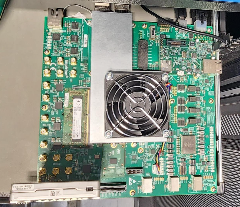
Agilex 7 F-Series SoC Development Kit with SSD End Point
Ensure your NVMe has a valid partition enabled.
Create SD Card for Agilex 7 F-Series SoC Development Kit
This section describes how to create a SD Card that contains the default pre-built version of this reference design.Creating SD card on Linux
- Extract sdimage.tar.gz file ( after extraction gsrd-console-image-agilex.wic should be seen)
tar xf sdimage.tar.gz
- Determine the device associated with the SD card on the host
cat /proc/partitions (Let's assume it is /dev/sdx.)
- Use dd utility to write the SD image to the SD card
sudo dd if=gsrd-console-image-agilex.wic of=/dev/sdx bs=1M
Note we are using sudo to be able to write to the card - Use sync utility to flush the changes to the SD card
sudo sync
Creating SD card on Windows
- Download the sdimage.tar.gz listed in the Release Contents section above.
- Run tar xvfz sdimage.tar.gz to extract the SD Card binary image (sdimage.img).
- Insert the SD Card to be updated into an SD Card reader attached to the computer.
- Use Win32DiskImager to write the image to the SD card.
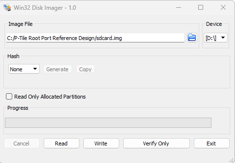
SD Card Programming using Win32DiskImager Tool
Replace kernel.itb in SD card with the PCIe root port enable kernel.itb
If you previously used FM 61 GSRD kernel.itb or other kernel.itb, replace it with the PCIe root port.- Download the PCIe root port kernel.itb from the Release Contents.
- Replace the kernel.itb in the SD with the PCIe root port enable kernel.itb.
Booting the System
Configuring Serial Connection
On Windows, utilities such as TeraTerm and PuTTY can be used to connect to the board. They are easily configured from the tool menus. On Linux, the minicom utility can be used. Here is how to configure it:- The virtual serial port is usually named /dev/ttyUSB0. In order to determine the device name associated with the virtual serial port on your host PC, please perform the following:
- Use the following command to determine which USB serial devices are already installed: ls /dev/ttyUSB*
- Connect mini USB cable from J7 to the PC. This will enable the PC to communicate with the board, even if the board is not powered yet.
- Use the ls /dev/ttyUSB* command command again to determine which new USB serial device appeared.
- Install minicom application on host PC, if not installed.
- On Ubuntu, use sudo apt-get install minicom
- Configure minicom.
sudo minicom -s
- Serial Device: /dev/ttyUSB0 (edit to match the system as necessary)
- Bps/Par/Bits: 115200 8N1
- Hardware Flow Control: No
- Software Flow Control: No
- Hit [ESC] to return to the main configuration menu
Programming *.sof file Using JTAG Configuration
- Please make sure switches on the Agilex 7 F-Series SoC Development Kit are configured as below.
- SW1: ON-ON-ON-ON
- SW2: All ON
- SW3: All OFF
- SW4: ON-OFF-ON-OFF
- With the board powered down, insert the SD Card created above into the SD Card slot.
- Connect miniUSB cable between host PC and miniUSB port (J7) on the board and connect mini USB cable between host PC and mini USB port (J7) on OOBE Daughter Card.
- Power on the Agilex 7 SoC Development Kit and open a serial port terminal application on the host PC such as TeraTerm, Putty, Minicom on host PC with settings below.
- Baud-rate: 115,200
- Parity: none
- Flow control: none
- Stop bits: 1
- Open Quartus Prime Programmer and select Agilex Si/SoC Dev Kit for the Hardware Setup.
- Click Auto Detect to detect the AGILEX_HPS device in the JTAG scan chain.
- Select the AGB014R24B device followed by selection of 10M16SA.
- Select the AGB014R24B device from the JTAG scan chain and click on Change File.
- Navigate to the location of the pre-built sof file and click OK.
- Check the Program/Configure checkbox. Click Start to begin configuring the device.
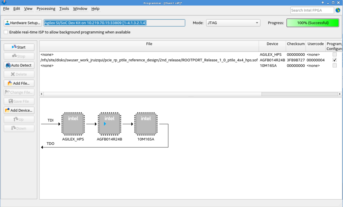
Programmer configuration
You should see the U-Boot bootloader start...
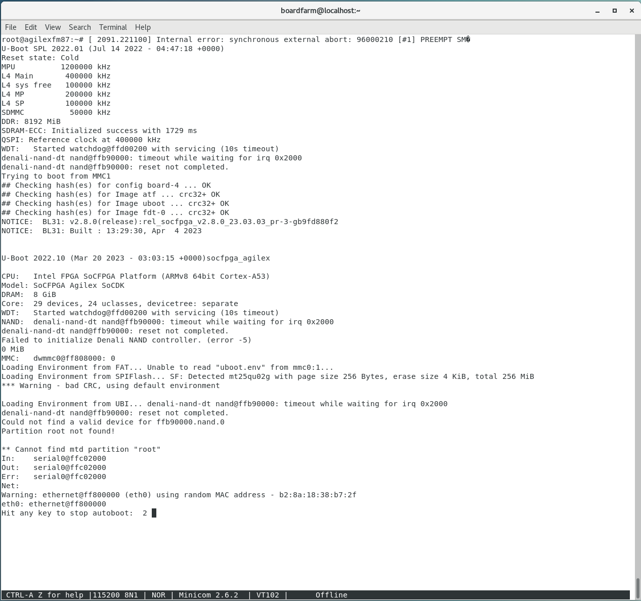 Once you programmed the Development Kit will start the boot up process, but that first run will not boot up correctly. Write on command line bootm to retry the boot up process you will see the system booting successful in Linux.
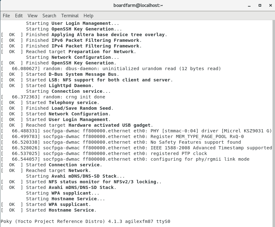 Once the system has booted into Linux, login by entering “root” as the username
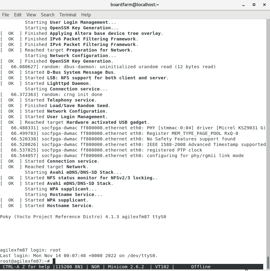
Discovery of Intel SSD End Point
Once logged-in as root, you can run “lspci -v” command to make sure the Intel SSD NVMe is discovered by the PCIe root port and the proper Linux kernel modules have been loaded. You should see the output as below.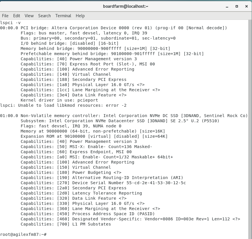
fio (flexible I/O tester) on NVMe
Once End Point is discovered, run fio (flexible I/O tester) test on NVMe with command below in Linux console.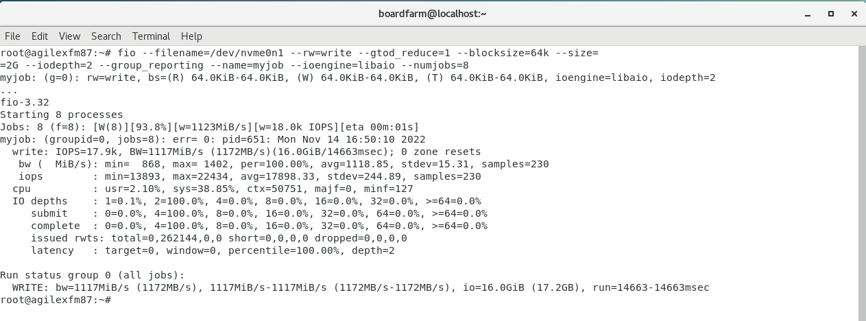 Run fio (flexible I/O tester) test on NVMe with command
 - Read fio command: fio --filename=/dev/nvme0n1 --rw=read --gtod_reduce=1 --blocksize=64k --size=2G --iodepth=2 --group_reporting --name=myjob --ioengine=libaio --numjobs= no of job
- Write fio command: fio --filename=/dev/nvme0n1 --rw=write --gtod_reduce=1 --blocksize=64k --size=2G --iodepth=2 --group_reporting --name=myjob --ioengine=libaio --numjobs= no of job
- fio --filename=/dev/nvme0n1 --rw=read --gtod_reduce=1 --blocksize=64k --size=8G --iodepth=2 --group_reporting --name=myjob --ioengine=libaio --numjobs= no of job
- fio --filename=/dev/nvme0n1 --rw=write --gtod_reduce=1 --blocksize=64k --size=8G --iodepth=2 --group_reporting --name=myjob --ioengine=libaio --numjobs= no of job
| Jobs | Write | Read |
|---|---|---|
| 4 | 1180MB/s | 1191MB/s |
| 8 | 1501MB/s | 1950MB/s |
| 16 | 1690MB/s | 2300MB/s |
| 20 | 1672MB/s | 2354MB/s |
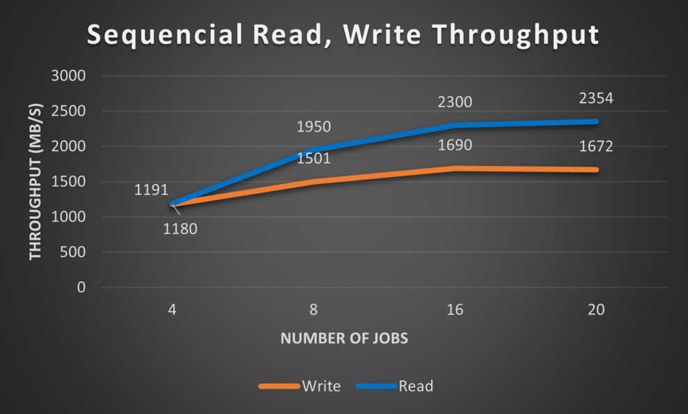
Intel SSD NVMe Write/Read Throughput
The picture above has the size value of 2G (--size=2G)
Rebuilding Source Files
The instructions below are optional. They show how to rebuild the software and/or hardware if you want to experiment with the reference design. This reference design is a modified version of the Golden System Reference Design, so please refer to GSRD for Agilex 7 F-Series - User Manual for more details regarding the build flow. It is highly recommended that you perform all the relevant compilation steps listed in in the user's manual before continuing. The following steps are only meant to be a minimal list. Please walk through the Build Flow of Golden System Reference Design (GSRD) User manuals to have more understanding.Rebuild Hardware Design
Retrieve the archive file ROOTPORT_SRD_HW_Release_3_0.tar.gz for the Release Contents, this containing the hardware design and save it in the home fold Rebuilding hardware design step, please refer to Setting up Environment.- Setting up Enviroment.
- Building the Hardware Design.
- You can rebuild the hardware via Intel Quartus Prime Pro GUI or CLI.
- If you refer to Agilex 7 Golden System Reference Design (GSRD) User Manuals to rebuilding, make sure the dir path is correct when you execute the command.
- Building Core RBF.
Rebuilding Source Files
Please refer to Compiling U-Boot FSBL and SSBL for instructions to compile Agilex 7 SoC U-Boot First Stage Boot Loader (FSBL) and Second Stage Boot Loader (SSBL).Build Agilex PCIe Root Port and Integrating U-boot FSBL
- The project is available here
- Follow the instructions listed at Compiling Hardware Design and Integrating U-boot FSBL to compile the hardware design and integrating the FSBL.
Compiling Linux
If you just want to compile Linux kernel and device tree only and re-use existing Linux Root Filesystem, please run steps below.- Download this patch to add PCIe root port node into socfpga_agilex_etile_4_channel.dtsi in ~/linux-socfpga/arch/arm64/boot/dts/intel/.
- Run commands below to apply the patch and build Linux kernel and Linux device tree.
$ wget https://developer.arm.com/-/media/Files/downloads/gnu/11.2-2022.02/binrel/gcc-arm-11.2-2022.02-x86_64-aarch64-none-linux-gnu.tar.xz
$ tar xf gcc-arm-11.2-2022.02-x86_64-aarch64-none-linux-gnu.tar.xz
$ export PATH=`pwd`/gcc-arm-11.2-2022.02-x86_64-aarch64-none-linux-gnu/bin:$PATH
$ export ARCH=arm64
$ export CROSS_COMPILE=aarch64-none-linux-gnu-
$ git clone https://github.com/altera-opensource/linux-socfpga -b QPDS23.3_REL_GSRD_PR
$ cd linux_socfpga
$ apply patch (Ex patch -p1 < SW/6_1_38_agilex7_pcierp.patch )
$ make defconfig ARCH=arm64 CROSS_COMPILE=aarch64-none-linux-gnu-
$ make menuconfig ARCH=arm64 CROSS_COMPILE=aarch64-none-linux-gnu- , add CONFIG_PCIEAER and required PCI EP drivers ( Ex CONFIG_BLK_DEV_NVME for nvme storage)
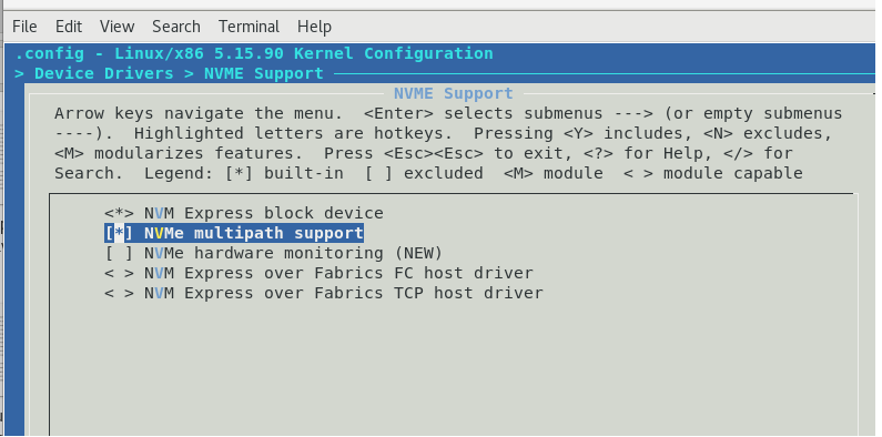
menuconfig
In kernel configuration, go to "Device Drivers" and input "Y" on "NVM Express block device". Save the changes to .config. Type "make" to compile the kernel.
$ make -j`nproc` ARCH=arm64 CROSS_COMPILE=aarch64-none-linux-gnu-
- kernel image should be avaliable at "arch/arm64/boot/Image"
- dtb file should be avaliable at "arch/arm64/boot/dts/intel/socfpga_agilex_socdk.dtb"
Generating the kernel.itb
Create kernel_itb folder and copy fit_kernelagilex_pci.its and file.rbf from release content info the kernel_itb folder.cd .. mkdir kernel_itb cd kernel_itb mv file.rbf agilex_gsrd_ghrd.core.rbf copy ../fit_kernel_agilex_pci.its and ../file.rbfCopy kernel image and file into kernel.itb folder
cp ../linux-socfpga/arch/arm64/boot/dts/intel/socfpga_agilex_socdk.dtb
cp ../linux-socfpga/arch/arm64/boot/Image
xz --format=lzma Image
Generate kernel.itb
mkimage -f fit_kernel_agilex_pci.its kernel.itb
Crafting Device Tree Manually for PCIe root port enablement
If you would like to add PCIe root port to your custom dts, PCIe root port bindings below can be added into the dts file.- Agilex SoC PCIe Root Port device tree descriptions
- PCIe controller dts node descriptions
- PCIe MSI controller dts node descriptions
soc {

                aglx_hps_bridges: bridge@80000000 {
                        compatible = "simple-bus";
                        reg = <0x80000000 0x20200000>,
                              <0xf9000000 0x00100000>;
                        reg-names = "axi_h2f", "axi_h2f_lw";
                        #address-cells = <0x2>;
                        #size-cells = <0x1>;
                        ranges = <0x00000000 0x00000000 0x80000000 0x00040000>,
                                 <0x00000000 0x10000000 0x90000000 0x10000000>,
                                 <0x00000000 0x20000000 0xa0000000 0x00200000>,
                                 <0x00000001 0x00010000 0xf9010000 0x00008000>,
                                 <0x00000001 0x00018000 0xf9018000 0x00000080>,
                                 <0x00000001 0x00018080 0xf9018080 0x00000010>;

                        pcie_0_pcie_aglx: pcie@200000000 {
                                       compatible = "altr,pcie-root-port-3.0";
                                       reg = <0x00000000 0x20000000 0x00200000>,
                                             <0x00000000 0x10000000 0x10000000>,
                                             <0x00000001 0x00010000 0x00008000>;
                                       reg-names = "Hip", "Txs", "Cs";
                                       /* p-tile
                                       port_conf_stat = <0x104000>;*/
                                       /* f-tile */
                                       port_conf_stat = <0x14000>;
                                       interrupt-parent = <&intc>;
                                       interrupts = <0x0 0x14 0x4>;
                                       interrupt-controller;
                                       #interrupt-cells = <0x1>;
                                       device_type = "pci";
                                       bus-range = <0x0000000 0x000000ff>;
                                       ranges = <0x82000000 0x00000000 0x00000000 0x00000000 0x10000000 0x00000000 0x10000000>;
                                       msi-parent = <&pcie_0_msi_irq>;
                                       #address-cells = <0x3>;
                                       #size-cells = <0x2>;
                                       dma-coherent;
                                       interrupt-map-mask = <0x0 0x0 0x0 0x7>;
                                       interrupt-map = <0x0 0x0 0x0 0x1 &pcie_0_pcie_aglx 0x1>,
                                                      <0x0 0x0 0x0 0x2 &pcie_0_pcie_aglx 0x2>,
                                                      <0x0 0x0 0x0 0x3 &pcie_0_pcie_aglx 0x3>,
                                                      <0x0 0x0 0x0 0x4 &pcie_0_pcie_aglx 0x4>;
                                       }; //end pcie@0x010000000 (pcie_0_pcie_aglx)

                          pcie_0_msi_irq: msi@10008080 {
                                       compatible = "altr,msi-1.0";
                                       reg = <0x00000001 0x00018080 0x00000010>,
                                             <0x00000001 0x00018000 0x00000080>;
                                       reg-names = "csr", "vector_slave";
                                       interrupt-parent = <&intc>;
                                       interrupts = <0x0 0x13 0x4>;
                                       msi-controller = <0x1>;
                                       num-vectors = <0x20>;
                                       }; //end msi@0x100008000 (pcie_0_msi_irq)
                        };
	};
};
Creating and Updating SD Card
The picture below presents the layout of the SD card that is used in PCIe root port GSRD.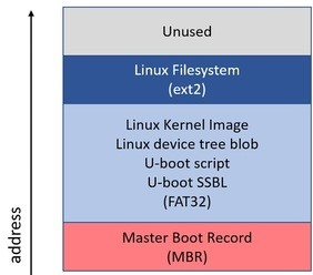 After loading the SDimage, the SD will have this documents
| File Name | Description |
|---|---|
| Boot.scr.uimg | U-boot script |
| Kernel.itb | Linux kernel image file |
| u-boot.itb | U-Boot FIT image |
© 1999-2024 RocketBoards.org by the contributing authors. All material on this collaboration platform is the property of the contributing authors.
This website is using cookies. More info.
That's Fine
 RocketBoards