- Home
- Documentation
- Community
- Projects
- Boards
- Agilex 5 SoC
- Agilex 7 SoC
- Arria 10 SoC
- Nallatech 385A - Arria 10 FPGA Network Accelerator Card
- Nallatech 385A-SoC Accelerator Card with Arria 10 FPGA
- ALARIC Instant DevKit ARRIA 10 SoC FMC IDK by REFLEX CES
- Altera Arria 10 SoC Virtual Platform
- Altera Arria 10 SoC Board
- Nallatech 510T compute acceleration card with Intel Arria 10 FPGA
- REFLEX CES Achilles Arria 10 SoC SOM
- Terasic Arria10 SoC Board : HAN Pilot Platform
- Arria V SoC
- Cyclone V SoC
- Altera Cyclone V SoC Board
- Arrow SoCKit User Manual - July 2017 Edition
- Arrow SoCKit User Manual - November 2019 Edition
- Arrow SoCKit Evaluation Board
- Atlas-SoC Development Platform
- Critical Link MitySOM-5CSx Development Kit
- Cyclone V Ethernet driver problems
- DE10-Nano Development Board
- Terasic DE10-Standard Development Kit
- Devboards DBM-SoC1 module
- Devboards DBM-SoC2 module
- EBV SoCrates Evaluation Board
- Enclustra Mercury SA1 SoC Module
- Enterpoint Drigmorn 5
- Enterpoint Larg 2
- Altera Cyclone V SoC Development Platform
- Mpression Helio SoC Evaluation Kit by Macnica
- Mpression Sodia Evaluation Board by Macnica
- ARIES Embedded - MCV System on Module
- Mpression Borax SOM Module and Development Kit by Macnica
- Enterpoint Mulldonoch 3
- Networked Pro-Audio FPGA SoC Development Kit by Coveloz
- NOVPEK™CVLite
- NOVSOM®CV
- NOVSOM®CVLite
- NovTech IoT Octopus™
- NovTech NetLeap™
- Enterpoint Raggedstone 4
- Solectrix SMARC compliant System-on-Module
- Terasic DE1-SoC Development and Education Board
- Stratix 10 SoC
- Find a Board
- News
Documentation
Similar topics
-
Update Preloader/U-boot on DE10-Nano using Windows 10 (WSL)
Update Preloader/U boot in 20.1 or later for Cyclone V SOC on Windows OS Development Machine
-
DE10-Nano Code Samples FFT
Code samples for FFT application that ships with the DE10 Nano board
-
DE10-Nano Code Samples GPIO
Code samples for the example design that ships with the DE10 Nano board
-
Mpression Borax SOM Module and Development Kit by Macnica
The Mpression Borax SOM is a system on module card integrating an Altera® Cyclone® V SoC FPGA and necessary memory, power and external interfaces on a very small size card and uses an Altera Cyclone V SoC FPGA tightly integrates two ARM Cortex A9 cores and FPGA fabric
-
 Cyclone V SoC GSRD
Cyclone V SoC Golden System Reference Design
Recent Changes
-
 Macnica Sulfur ~ Development Kit for Agilex™ 5 FPGA E-Series ~
-
 Building Bootloader for Agilex 5
Building latest bootloaders for Agilex 5 SoC Devices
 - Ashling RiscFree Examples
-
 GSRD for Agilex 7 I-Series Transceiver-SoC DevKit (4x F-Tile)
Golden System Reference Design for DK SI AGI027FB, DK SI AGI027FA and DK SI AGI027FC
 -
Intel® Simics® Simulator for Intel FPGAs Release Notes
This page provides release information about the Intel® Simics® simulator for Intel FPGAs.
Table of Contents
Overview
The DE10-Nano development board features a Cyclone® V SoC FPGA combined with a wide range of peripheral devices and I/O expansion headers to create a powerful development platform. This low-cost kit serves an interactive, web-based "guided tour" that lets you quickly learn the basics of SoC FPGA development and provides an excellent platform on which to develop your own SoC FPGA design. Cyclone V SoCs integrate a dual-core ARM® Cortex®-A9 MPCore™ hard processor, peripherals, and memory interfaces with FPGA fabric using a high-bandwidth interconnect backbone. They combine the performance and power savings of a hard processor system (HPS) with the flexibility of programmable logic.Board Photos
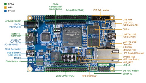 (click to enlarge)
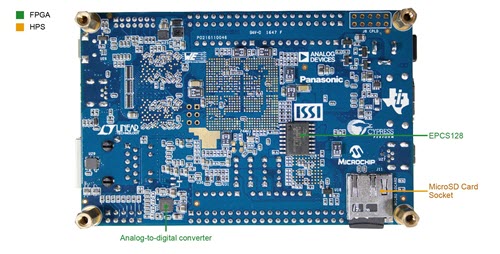 (click to enlarge)
Board Block Diagram
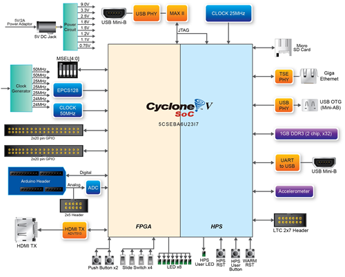 (click to enlarge)
System Block Diagram
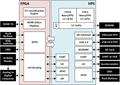 (click to enlarge)
Kit Features
The DE10-Nano Development board features the following:- Cyclone V SE development board
- Featured devices
- FPGA configuration sources
- Embedded USB-Blaster II (JTAG) cable
- Serial configuration flash - EPCS128
- Hard processor system (HPS)
- FPGA I/O interfaces
- x2 push buttons
- x4 slide switches
- x8 LEDs
- Three 50MHz clock sources from the clock generator
- Two 40-pin expansion header with diode protection
- One Arduino expansion header (Uno R3 compatibility), can connect with Arduino shields.
- One 10-pin Analog input expansion header. (shared with Arduino Analog input)
- 8-channel, 12-bit A/D converter, 500ksps 4-pin SPI interface with FPGA
- HDMI Output
- Hard Processor System (HPS)
- 800MHz Dual-core ARM Cortex-A9 processor
- 1GB DDR3 SDRAM (32-bit data bus)
- x1 Gigabit Ethernet PHY with RJ45 connector
- x1 USB OTG port, USB Micro-AB connector
- Micro SD card socket
- 1 8GByte SD Card flash
- Accelerometer (I2C interface + interrupt)
- UART to USB, USB Mini-B connector
- Warm reset button and cold reset button
- One user button and one user LED
- LTC 2x7 expansion header
- Embedded software
- Linux kernel 4.1.33 LTSI
- Angstrom 2016.12
- FPGA hardware design
- 32-bit Fast Fourier Transform engine (FFT)
- HDMI output (video pipeline)
- General-purpose I/O (GPIO) for LEDs, push buttons, and slide switches
- SPI master interface to A/D converter
- I/F to Arduino shield headers (digital I/O, serial I/O, A/D converter)
- GPIO
- SPI master
- I2C Controller
- UART
Arduino Header
The board provides Arduino Uno revision 3 compatibility expansion header which comes with four independent headers. The expansion header has 17 user pins (16pins GPIO and 1pin Reset) connected directly to the Cyclone V SoC FPGA. 6-pins Analog input connects to ADC, and also provides DC +9V (VCC9), DC +5V (VCC5), DC +3.3V (VCC3P3 and IOREF), and three GND pins.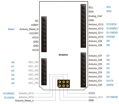 (click to enlarge)
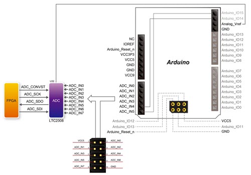
In addition to the 16 pins for digital GPIO, there are also 6 analog inputs on the Arduino Uno R3 Expansion Header (ADC_IN0 ~ ADC_IN5) which are connected to an analog-to-digital converter (Linear Technology LTC2308). The LTC2308 is a low noise, 500ksps, 8-channel, 12-bit ADC with a SPI/MICROWIRE compatible serial interface. It can be configured to accept eight input signals at inputs ADC_IN0 through ADC_IN7. These eight input signals are connected to a 2x5 header, as shown below.
Analog Connections
 (click to enlarge)
2x40 Pin Headers
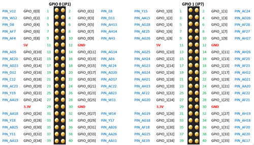
The board has two 40-pin expansion headers. Each header has 36 user pins connected directly to the Cyclone V SoC FPGA. It also comes with DC +5V (VCC5), DC +3.3V (VCC3.3), and two GND pins. The Figure below shows the I/O distribution of the GPIO connector. The maximum power consumption allowed for a daughter card connected to one or two GPIO ports is as follows:- 5V: 1.0A (depending on the power adapter specification)
- 3.3V: 1.5A
 (click to enlarge)
Resources
- DE10-Nano Getting Started Guide
- Instructions and source files to rebuild the FPGA project
- Instructions for rebuilding the Linux BSP
- GPIO Example Design
- FFT Example Design
- Accelerometer Tutorial
- Extend the rootfs Partition
- Open PacKaGe management (OPKG)
- Build and install the MRAA and UPM libraries
© 1999-2024 RocketBoards.org by the contributing authors. All material on this collaboration platform is the property of the contributing authors.
This website is using cookies. More info.
That's Fine
 RocketBoards